Project overview
What is the purpose of the circuit designed in this project?
The purpose of the circuit is to understand the hands on experience of creating a complex breadboard, but to also build a circuit that can display your date of birth.
What are the constraints on the design?
Everything is by hand, and it requires a lot of logic which results in a tiny bit of a mistake can cause hours of troubleshooting. The constraint is that it can only display one date of birth and requires a lot of focus and time. As well as the Boolean Algebra as it requires me to go back a lot and limits my ability to configure as efficiently as possible.
truth table
What is the purpose?
The purpose of a table is to display where and how everything will work in terms of what will trigger which segments to be on and what will remain off. It is the period of planning my circuit.
The purpose of a table is to display where and how everything will work in terms of what will trigger which segments to be on and what will remain off. It is the period of planning my circuit.
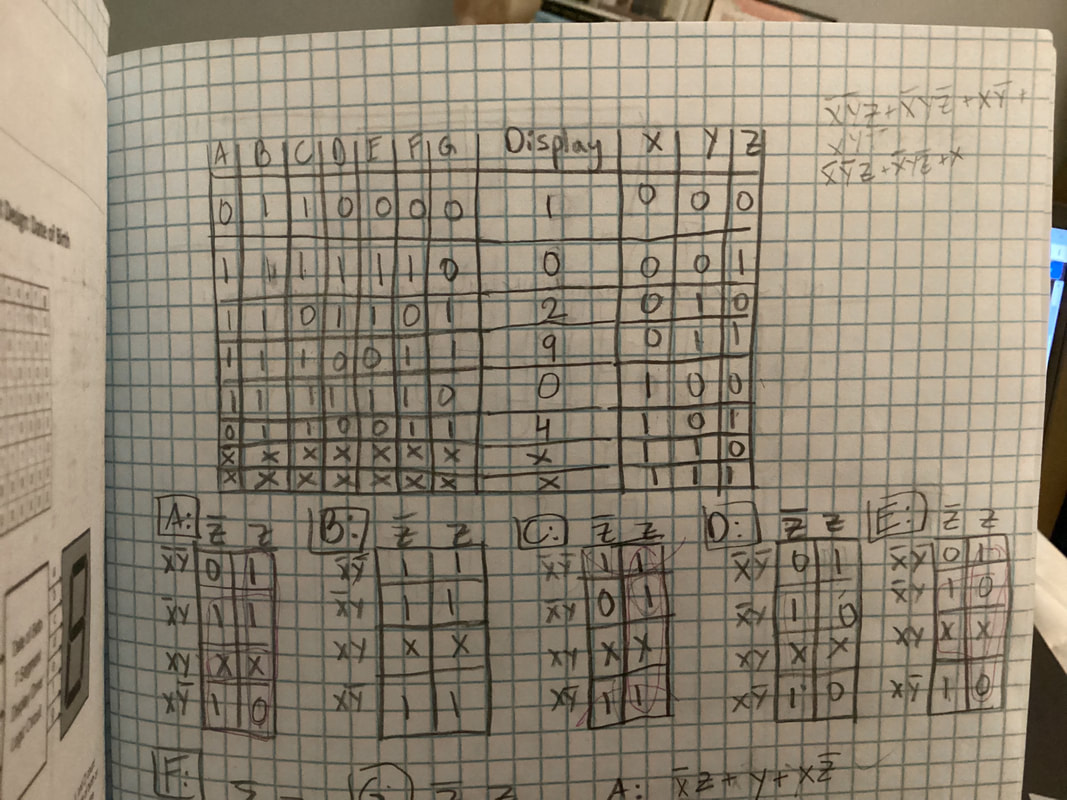
Why do we have A-G columns? What does X mean?
We have "a" to "g" columns since we have 7 segments that are represented from "a" to "g" and the columns express what each segment will represent with the 7-segment-display. The segments "a" to "g" each is a segment that makes up from 0 to 9. The X essentially means that it does not matter whether it is a 0 or 1 as it will work for both.
We have "a" to "g" columns since we have 7 segments that are represented from "a" to "g" and the columns express what each segment will represent with the 7-segment-display. The segments "a" to "g" each is a segment that makes up from 0 to 9. The X essentially means that it does not matter whether it is a 0 or 1 as it will work for both.
k-mapping and simplified expressions
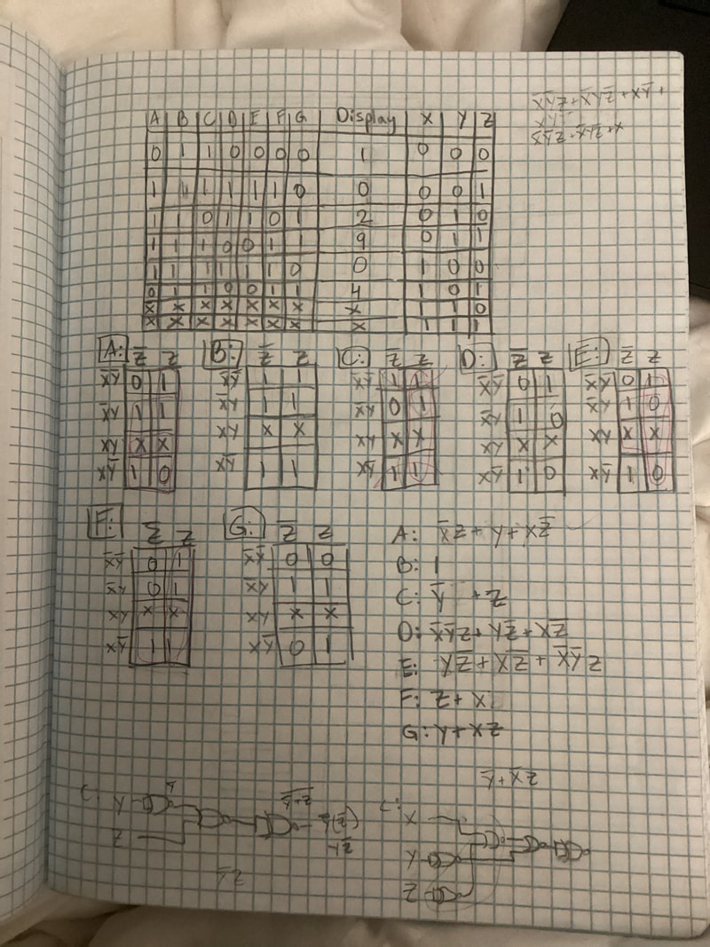
K-mapping is in sums of Products form. By using my K-maps and simplifying the most that I can, I end up with these minterms for my circuit. K-mapping is a quicker and more logical way to simplify minterms compared to Boolean Algebra. Boolean Algebra creates more likeliness for mistakes compared to K-maps as well as K-maps are simplistic and organized compared to Boolean Algebra. We have seven segments and each segment needs their own minterms, so having different minterms could seem like a lot but when separated to their segments, it is a lot more clear and you will see that it is not a lot of expressions compared to unsimplified expressions.
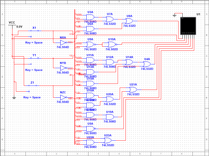
multisim
Gates |
Number of Gates Required |
Number of Chips Required |
AND |
11 |
3 |
OR |
7 |
2 |
NOR |
2 |
1 |
NAND |
1 |
1 |
INVERTERS |
3 |
3 |
We use NAND or NOR gates since they can be any AOI gates, and that is helpful since they are also cheaper than AOI gates. Some of the minterms used less gates when I changed the gates to NOR or NANDs, but some had less gates with AOI gates. The ones I changed to NOR or NANDs used less chips since it was all on one chip instead of AOI chips. I would say about 2 chips were not used when we switched some of the segments to NOR or NANDs. It is important because it saves space and money when we need to configure gates.
Seven-Segment Displays:
It displays seven segments to make up from numbers 0-9 that uses logic to configure the segments. A common cathode requires a ground, and the segments will be powered high. And a common anode is the inverse, it requires a power high and the segments will be grounded. I am using a common cathode simply because it is easier on me to configure as it is powered with the segments and itself is grounded. The purpose of a resistor is to limit the current of the positive charge that will prevent the LEDs from burning out, the common value of a resistor is 220 ohms.
It displays seven segments to make up from numbers 0-9 that uses logic to configure the segments. A common cathode requires a ground, and the segments will be powered high. And a common anode is the inverse, it requires a power high and the segments will be grounded. I am using a common cathode simply because it is easier on me to configure as it is powered with the segments and itself is grounded. The purpose of a resistor is to limit the current of the positive charge that will prevent the LEDs from burning out, the common value of a resistor is 220 ohms.
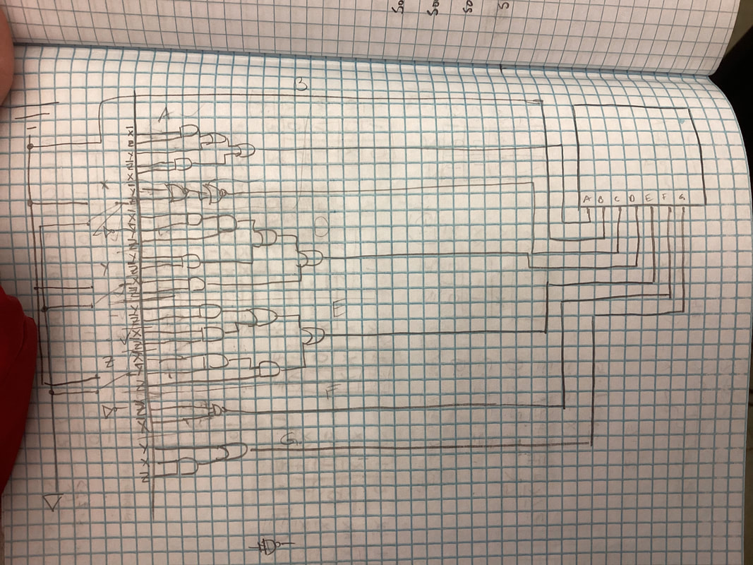
I used a NOR gate for segment “c” and used NAND gates for segment “f” since they had expressions that allowed NOR and NAND gates to require less gates for the same output.
Tinkercad
My breadboarding experience was really frustrating as the segments required individual focus and any subtle mistake could cause havoc on the outputs of the breadboard. In the end, it was an intense but slow burn of a satisfying feeling as I was able to do it by myself and figure out the puzzling problems before I went crazy. I made many mistakes, especially on segment C, D, and E. With E and D, I struggled the most since I was trying to create a shortcut with my project by using a combination already used in another segment which ended up taking more time to troubleshoot rather than making another logic combination. Since I struggled with those, it required many overviews of every aspect of the project even if I was confident with my answers. Overall the skills I have developed was the ability to go back and start over at scratch even going as far as pinpointing what specific logic created a certain output and to eliminate my own human error. It was also very important to be able to organize the gate layout properly to ensure space for the rest of the circuit since it took up so much space. The troubleshooting was not too difficult, it just required an immense amount of patience, especially when you were on a time constraint and you were trying to rush. My troubleshooting was frustrating to a degree when I mistook my X for my Z and used the wrong gate because I did not look and double check. I have realized that troubleshooting is a skill that people have to develop in this field considering that is at least 50% of the job.
Bill of materials
Components |
Quantity |
AND |
2 |
OR |
2 |
NOR |
1 |
NAND |
1 |
Inverter |
1 |
Wires |
Lots Required |
conclusion
I learned from this project how to trouble shoot and to maintain patience since it is always a mistake that I make, as I cannot really blame anyone else but myself. I learned how to double check my work in terms of going back from physical wires to K-mappings. I would say next time I should label my X, Y, and Z components so I do not mix them up again. As well as leave notes as to what I did the last time so I will remember where I left off instead of forgetting my progress. My questions are more as how is this practical for this type of configuration as we can use integrated circuits and essentially change it any time for minimal costs?
